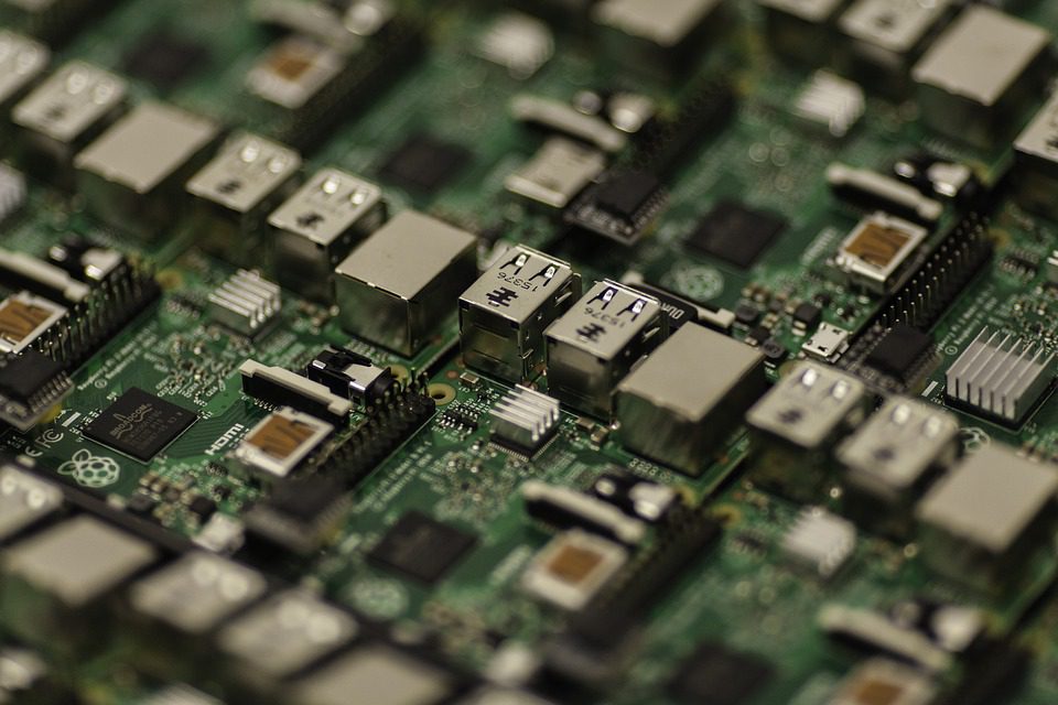
A printed circuit board, or PCB, provides mechanical support and connection to electronic components through the use of conductive tracks, pads, and other features that are etched from copper sheets and laminated onto a substrate that does not conduct electricity. PCBs may be single sided, double sided, or multi-layered. PCBs today may contain capacitors, resistors, and other components that are embedded in the substrate.

(Pixabay / Pexels)
Printed circuit boards are used in most electronics products. Those that do not use printed circuit boards employ point-to-point construction or wire wrap. The manufacture of PCBs has been automated, enabling mass production.
Before printed circuit boards became the norm in electronics production, the industry relied on point-to-point construction. This technique resulted in unreliable designs and bulky products that required large sockets. These problems were eliminated when printed circuit boards became part of regular electronics production.
The early concept of PCBs surfaced in the 1920s. The boards were made of Bakelite, Masonite, or plain pieces of wood. People drilled holes in the boards and riveted them with brass wires. They were ugly, bulky contraptions, but they introduced a new concept with countless possibilities.
The first double-sided PCB with plated through holes was introduced in 1947. The use of resins and other materials became popular during the 50s and 60s. PCBs of this generation were printed only on one side with the electrical components on the other side. This type of PCB was seen as a great improvement compared to the unwieldy wired mechanisms of the past.
In 1956, a patent was granted to a group of U.S. Army scientists for the process of assembling printed circuit boards, marking a big step forward for the industry. The process required making wiring pattern drawings and rendering a photograph onto a zinc plate. This plate was then used for offset printing. The wire was printed in acid-resistant ink on copper foil and later etched with an acid solution.
The first multi-layer PCBs were produced in 1960. The PCBs became smaller in the 1970s, thanks to the introduction of the hot air soldering method. The manufacture of PCBs further improved during the ‘80s, with surface mount parts becoming the preferred option over through-hole components. This move further reduced the size of the PCBs but added more functionality.
The use of multi-layered PCBs in the ‘90s lowered the cost of production. Demand for PCBs continues to increase as the electronics market evolves. In many ways, PCBs have become the backbone of the electronics industry.
