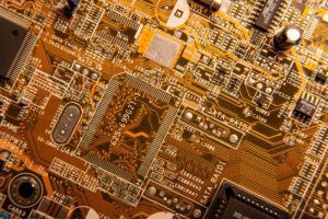
Ever heard of an 8-layer PCB? It’s the Beyoncé of circuit boards – a popular choice with plenty of benefits to boot. Sure, like any superstar, it’s got its flaws, but it’s still the go-to pick for various purposes. In this article, we’re diving deep into the world of 8-layer PCBs – from design considerations to finding relevant manufacturers and more.

(freepik/Freepik)
What is an 8-layer PCB?
An 8-layer PCB boasts a generous serving of conductive copper layers, all snuggly nestled between insulating materials. These layers are connected via some neat holes in the board called vias. Their purpose? To bring electronic components together for improved performance. With all that routing space and via real estate, this multilayer PCB is perfect for applications that demand multiple power islands.
An 8-layer PCB is also reliable and sturdy, with a firm stack-up that ensures mutual connections. And with more planes than your average PCB stack up, this kind of circuit board excels in EMC performance. Those extra layers aren’t just for show, though; they also help improve PCB routing and various other functions.
Why use the 8-layer PCB stack-up?
An 8-layer PCB stack-up just makes sense in some cases. You can use it to achieve better ground plane separation and power, improved EMC shielding, and enhanced high-speed signal routing. Rest assured, your everyday, run-of-the-mill circuit board can’t deliver such results, even if you integrate additional components.
Other benefits of using an 8-layer PCB stack-up over lower-layer circuit boards include:
- Lower radiation: The 8-layer PCB variety has superior signal integrity, which helps to lower radiation emission.
- More reliability: The improved signal integrity and power distribution make the 8-layer PCB more reliable than its lower-layer counterpart.
- Better power distribution: Using inner layers, an 8-layer printed circuit board can deliver improved power distribution.
- Greater affordability: With less material used and higher manufacturing efficiency, 8-layer PCB costs assemblers less than lower-layer circuit boards.
Materials used in an 8-layer PCB stack-up
8-layer PCBs feature a stack of alternative conductive and dielectric layers. Some of the commonly used conductive materials in this PCB assembly are:
- Copper: This is the most common material present in 8-layer printed circuit boards. Besides its relatively low cost and excellent conductivity, copper is known for being cheap to recycle for users.
- Gold: While gold might not be as popular as copper for conductive material in 8-layer PCBs, it’s still a great choice thanks to its excellent conductivity, albeit at a higher cost
- Aluminum: Although not popular as copper or gold, aluminum is a solid choice for carrying high current traces in 8-layer PCBs. Those traces are typically thick with a low impedance, so you need a material that can handle the heat and current without breaking the bank.
As for substrate materials, we have:
- Polyimide: This is a popular choice for dielectric material in 8-layer PCBs thanks to its low dielectric constant and loss tangent. It’s great for high-frequency applications and high-temperature environments.
- FR-408: Another popular dielectric material for 8-layer PCBs, FR-408 has a lower dielectric constant and loss tangent than polyimide. It’s a good choice for high-speed digital applications.
- Arlon AD2000: This is another dielectric material with a very low dielectric constant and loss tangent. It’s a standard choice for 8-layer PCBs.
- Rogers RO400: With a very low dielectric constant and loss tangent, Rogers RO400 is a popular choice for 8-layer PCBs. It’s great for high-frequency and high-speed applications.
8-layer PCB design best practices
There’s a common misconception that an 8-layer PCB is the be-all and end-all of EMI issues. Sorry to burst your bubble, but that’s simply not true. As a PCB designer, you must consider certain factors to ensure your 8-layer stack-up performs at its best.
Impedance Control
Let’s start with impedance control. It’s a crucial aspect of successful 8-layer PCB design. The designer must measure the impedance of some traces during the design process. By matching the properties of the substrate material with the trace’s dimensions and locations, you can achieve impedance control. Be sure that the signal’s impedance is within the specified value. Trust us, it’ll pay off in terms of board performance.
Signal Shielding
Shielding signal layers from each other is a must for any 8-layer PCB manufacturer. Doing so prevents signal loss and infractions, which is why designers prefer 8-layer PCBs. More planes mean more shielding for signal layers.
Layers Balancing
Balancing the layers is another important consideration for 8-layer stack-up fabrication. Neglecting it can compromise the stackup’s functionality.
Preventing Noise Decoupling
Noise decoupling is a big no-no in an 8-layer stack-up design. The best way to prevent it is by creating a digital ground plane. This will help design multiple ground and power planes, which can then be deployed through the stack-up.
To sum up, the design and fabrication of an 8-layer PCB stackup requires attention to detail and adherence to important design techniques. Impedance control, signal shielding, prevention of noise decoupling, and layer balancing are all crucial to achieving a functional 8-layer board. Additionally, considerations such as stackup measling, interlayer offset, core materials, and bow and twist should not be overlooked during the fabrication process.
An EMS service provider who specializes in the manufacturing of multilayer boards is equipped to handle the intricacies involved in producing high-quality, 8-layer PCB stackups. With the use of different types of vias and surface finishes, they can ensure that the final product meets the required standards for EMC performance and signal routing.
As the electronics industry continues to evolve, the demand for high-performance 8-layer PCBs will only increase. PCBA manufacturers and EMS service providers who can design and fabricate these stack-ups with efficiency and accuracy will remain at the forefront of the industry.
