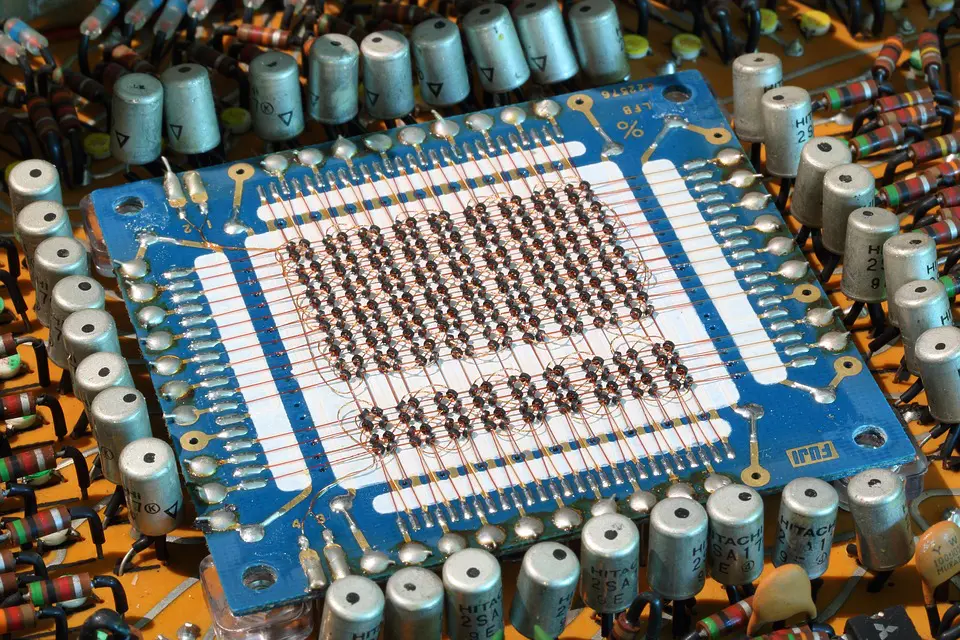
Just as legends and text help to make sense of streets and roads on a map, the silkscreen used in PCBs helps users understand the location of components, details for their orientation and placement, labels, logos and identifiers. The silkscreen’s layer houses information about the PCB assembly process. Essentially a detailed silkscreen can help both the engineer and the manufacturer to identify and locate all the PCB components, warning symbols, date codes, company logos, and part numbers.

(Pixabay / olafpictures)
How Is Silkscreen Applied?
Several years ago, silk screen was applied with the use of a stencil that helped apply ink onto the surface of the board. Today, the silk screening process utilizes manual screen printing, Direct Legend Printing (DLP) and Liquid Photo Imaging (LPI) instead. Here’s a quick overview of these three processes.
Manual screen-printing
This is the most cost-effective procedure for silk screening. Manual screen-printing makes use of epoxy ink to carry out the process, which is pushed onto the laminate and then dried to create an impression on the circuit board. The setup of this process is easy as well. The only downside is that manual screen-printing requires additional impression drying and board spacing. This is because of the bigger text size that can be achieved by using this method.
Direct Legend Printing (DLP)
The functions involved in this process are the same as those leveraged by paper printers. Inkjet printers that are capable of transferring ink on the printed circuit board are utilized for DLP. Another benefit of using this process is that the application data of CAD is directly printed on the PCB. Plus, the ink used in the DLP process is often upgraded to acrylic in order to minimize the impression drying time. Additionally, the digitalized process has the best time efficiency and the highest accuracy of all silk screening processes.
Liquid Photo Imaging (LPI)
Liquid Photo Imaging offers more accuracy than manual-screen printing. Liquid epoxy is used to coat the laminate. This epoxy has the characteristics of photo imaging. The silk screen’s sketch is then transferred to plates via exposure to ultraviolet (UV) light. The outcome that is achieved has a better precision than the manual silk-screening procedure. Also, LPI utilizes the board space more effectively. However, this process of silk screening demands more ink than the previous two processes. Moreover, the time to set up the process along with the application procedure is much higher. With that said, it’s the ideal method to use if you’re looking to save space on your PCB along with fineness for your work.
Implications of Silk Screening in PCB Assembly
When it comes to the PCB assembly process, the silk screen is used for the placement of parts. The markers of the silk screen help to provide accuracy to the housing process.
These markings may include polarity indicators (indicate the orientation of polarized parts), Pin 1 indicators (show which pins connect with different pads of the footprint), component outlines (establish where the components are to be fixed), and reference materials (help to determine component types from BOM (bill of materials).
For basic components with fewer pads, the component outline isn’t necessary but will be required for general placement. However, pin 1, polarity and reference indicators are crucial and cannot be neglected. Otherwise, you could end up with misplaced components.
Is Silk Screening Useful for PCB Testing?
In a word: Yes. Silk screening can be used to provide the technician or engineer with insight into the location where measurements are required during the troubleshooting and testing process. This can help to identify the causes of potential failures, as well as the verification of end performance.
Common silk screen markings used for troubleshooting or testing include warning symbols (help indicate parameters that should be handled with care or avoided), part numbers (offer device information and are handy in the absence of a datasheet), and test points (indicate locations where desired values are present).
Overall Importance of PCB Silk Screens
A well-made silk screen plays a very critical role as it can help reduce both the chances of PCB errors as well as the time taken to identify different vulnerabilities. This applies to both assemblies as well as the rework processes. Also, it isn’t always necessary for silk screening to spot all the passive parts that make up the devices on the PCB.
Instead, it’s okay if the silk screen mentions the functionality of the circuit. In fact, for PCBs packed with various tiny components, this is a much more achievable task than labeling every separate component. And while you can label the active components, the passive ones don’t need to be labeled. Opting to identify the functionality of the circuit rather than all the passive components will ensure that the legend of the PCB is legible as well as useful.
Conclusion
PCB silk screen is not only a technical process which can affect the entire quality of your circuit board, but it can also deliver value through elegant design. A good understanding of the procedure, along with the pros and cons of each silk screening technique, makes it easier to determine whether you’d want to do this yourself or choose a silk screening specialist for the procedure. In the former case, you’d need to know how to use a CAD solution for PCBs as well as how to design the font, color, and placements of text. Attention to detail is a must.
