There are many means of testing newly constructed PCBs. Checking by eye or using in-circuit testing are great ways to ensure that everything is where it should be. But these tests all require you to have access to the surface of your board. What about if you can’t see your components?
For more complex, multilayered boards, testing is much more challenging. Layers of boards and complex arrangements of chips will deny you the ability to see or probe individual components. Fortunately, for those who are fed up with relying on the “hoping it’s all ok” system, an alternative has been created: Boundary-Scan Tests.

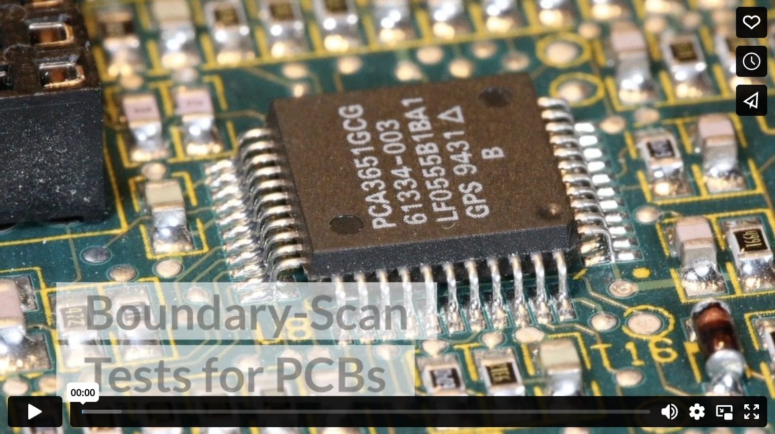
(PublicDomainPictures / pixabay)
What Are Boundary-Scan Tests?
Hardware interfaces that allow chips to be tested using a specific set of test signals are codified in the Joint Test Action Group (JTAG). This is a set of procedures and board architecture that were developed with Intel’s 80486 microprocessor. The IEEE 1149.1 (as these tests are known) has become the industry standard test for debugging all embedded systems.
This set of tests is designed to identify any faults in the complex programmable logic devices (CPLDs) or field-programmable gate arrays (FPGAs), which make up an integrated circuit (IC) package. According to IEEE 1149.1 architecture, you limit the number of manageable inputs available on the board by building the IC. This helps to remove some of the post-manufacturing testing procedures by integrating test logic into the IC itself.
This test logic tests the board’s electrical functionality; it can also help diagnose physical faults in the component interconnects. Before boundary-scan tests, the only way to identify faults within a compound PCB was through a costly x-ray scan. Now, testers can diagnose physical faults with pads, pins, and soldered BGA connections without looking inside the board.
IEEE 1149.1 architecture places a daisy chain of JTAG access ports (TAPs) around the outside of the board. These ports allow you to input data to the board and test for faults without looking inside the board itself. This system requires certain test bus connectors to be installed, and it is important to structure your board to incorporate them.
As JTAG technology rises in popularity for “interconnect” testing on PCBs and conducting ICs’ in-system programming (ISP) on those circuits, a growing number of EMS solution providers are providing ways to characterize JTAG-compliant components and devices. Those new to boundary-scan testing should look for solutions that offer DFT (design-for-testability) rules to analyze the device interconnections without needing advanced programming code quickly.
Advantages of Boundary-Scan Testing
Some of the benefits of boundary scan include:
- Reduces PCB testing costs, time, and efforts without affecting the quality. The tester also benefits from better coverage, reusable test patterns, and shorter time-to-release.
- Ability to test PCBs with no or limited access to internal pins and connections.
- Minimizes the risk of physical damage to the pins, circuit board or creating shorts via mechanical probes.
- Offers low cost in-circuit programming and debugging of the Flash, serial EEPROMs on-chip memory, CPLDs, etc.
- Incorporating JTAG cells at the board level eliminates the need for other expensive testing equipment while improving production and field testing.
Component Selection for JTAG
Planning your board to enable boundary testing will require you to include a specific set of components. Their specific placement will also help determine the layout of the rest of your board. As the name suggests, boundary testing will require you to ensure you have TAPs around the edge of the board itself.
Boundary-Scan Compliant Components
Most parts will be fed through your test bus connectors to allow you to run the tests, and you will need to make sure that your components are IEEE 1149.1 compliant. Most VLSI integrated circuits have already been designed with this in mind, giving you much more to work from. However, not all smaller chips are designed this way, or they may have been designed for JTAG to be optional. Make sure you properly research your intended components for IEEE 1149.1 compliance before you attempt to use them.
Dual-Function Components
Some components have been designed to allow dual functionality. In these cases, it’s best to avoid using the parts even if the JTAG is assisted in their function. Keeping parts simple is always the best option.
Check IEEE 1149.1 Instruction Support
Just because parts are boundary scan compatible, this does not mean they will support the correct instruction sets. Ideally, all the devices you use for your IC will need to be able to run SAMPLE / PRELOAD, EXTEST, and BYPASS commands. Though a component may support boundary scan, it may not support these commands. As they are mandatory command sets for an IEEE 1149.1 architecture, you must ensure that your parts support them. It is also a good idea to pick components that can support HIGHZ and IDCODE commands.
External Boundary Scan Description Language Files
JTAG components must also include the BSDL (External Boundary Scan Description Language) files provided by the vendors. These describe component capabilities, package information, implementation process, boundary scan behaviors, design warnings, scan-cells available, and more.
JTAG boundary-scan testing makes good sense for increasingly dense circuits and components. Today, it’s common to see JTAG logic and boundary-scan circuitry being incorporated into highly integrated circuits like FPGAs and microprocessors to help conduct measurements on PCBs with those components. At EMS Solutions, we’re proud to offer boundary-scan testing as part of our PCB assembly and testing solutions. This allows us to check interconnects and ICs on PCBs effectively and affordably.
Video