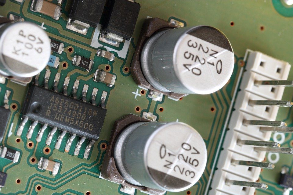
DC-DC buck converters help regulate DC output voltage so that it’s lower than the DC input voltage. Using these circuits is more power-efficient than using a linear regulator. Semiconductor manufacturers, therefore, are investing in innovative production processes that support the integration of a DC-DC converter IC die into a single module and various other components.

(Pixabay / olafpictures)
That being said, poor PCB layout can result in increased sound that negatively influences the output switching signal. In fact, it may reduce the overall efficiency of your regulator. Even if the component values and the circuit diagram are in order, improper PCB layout will hinder the regulator’s capability to deliver the correct operation.
Fortunately, these problems can be avoided through an appropriate board layout. Below are some benefits of a suitable PCB layout:
- Helps reduce circuit area as well as the clutter between different areas of the circuit
- Enhances circuit efficiency, voltage regulation, and thermal management
- Allows control over output switching signal and induced sound
Now that you know some idea of its benefits, let’s take a look at the things to consider when designing a PCB layout for a DC-DC buck converter.
Routing
When it comes to the crucial paths of routing, it’s best to keep inductance low. This can be achieved by minimizing the paths’ length instead of their widths. If every power component is on the same layer, there won’t be a need to via connections through the circuit board.
Routing paths’ corners should be maneuvered at a 45- degree angle (or rounded, if possible). Additionally, a separate ground for the power components that’s further away from the ground of the remaining components is recommended.
Because power components give off a lot of sound, it’s a good idea to contain them in a separate ground. You can then join the two ground paths together at a single point, perhaps to the thermal pad beneath the IC. The vias in the pad link the ground to the rest of the board.
Current Loops
The 3D layout of the on-state and off-state loops (found in the currents) is also vital. Based on Ampere’s law, the current flowing in physical loops creates a magnetic field in relation to the loop area and the current. This field then couples at higher frequencies by joining other circuit loops.
Hence, the 3D geometry should be set in such a way that there’s a minimum enclosed area between the loops. The best way to do this is to make the return path “collinear” to the outbound path. The preferred result for the circuit board will be return and outbound currents flowing in known, orderly paths.
Placement of Components
The key to a good PCB layout is to fix the components in the right locations. Many PCB designers make the mistake of fixing them for orderly and neat spacing rather than for the best circuit flow, which results in an ineffective converter layout. A better option is to keep the power components near the IC (once it’s fixed to the board).
For example, the input capacitor should be kept on the same surface layer as the IC pins it shares a connection with. When the opposite board side houses the capacitor, voltage noise could be generated by the via’s inductance used for connecting it with the IC.
Also, to lower radiated EMI, the designer should place the inductor on the same surface layer and as close to the IC as possible.
When it comes to the output capacitor, the placement should be close to the circuitry’s inductor. This will ensure that there’s minimal routing difference, which is key to achieving a good output voltage regulation. Lastly, small-signal components like decoupling and soft-start capacitors should be fixed close to the IC so they can directly route into it.
Thermal Factors
PCB layout for DC-DC buck converters is also driven by the thermal pad for the IC. The pad’s size and the number of vias, the quantity of layers, airflow, and max ambient temperature all need to be taken into consideration. At one point or another, an external heatsink would be required for the MOSFETs (metal oxide semiconductor field effect transistors). A MOFSET is a device with four terminals that is used for switching and amplifying electronic signals in electronic devices.
Conclusion
The performance of the power on the final printed circuit board will depend on the foundation of the buck converter circuitry. This small portion of the design doesn’t get much attention even though it’s critical for the overall layout. Minimize the connections by keeping the parts close to each other. Develop the ground routing of the layout (sensitive circuits thrive on a clean ground) so that return paths don’t push loud currents through the circuit. Time invested in the PCB layout is well worth it, especially when you consider the hours you could be spending fixing a poorly designed circuit.
