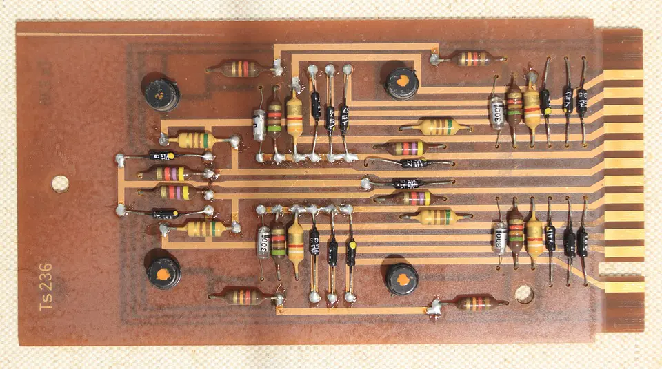
Technology makes the world go round, and it’s advancing at breakneck speed. Printed circuit boards are quickly becoming more detailed and complicated. On the horizon, there’s talk of smartphones using uber-efficient, “substrate-like PCBs” for motherboards. This will allow designers to put a bigger battery in the phone. Where the Internet of Things is concerned, PCBs are expected to help with security. Gadgets like Amazon Echo and Google Home depend on constant gathering and transmission of data, opening up more opportunities for hacking. The circuitry of new PCBs is being designed to assist with security measures.

(Pixabay / olafpictures)
Exciting new developments such as these raise the bar for printed circuit board assembly and production. The key to first-rate PCB output starts with the prototype layout. As you strive for more efficient designs to keep pace with new demands from consumers, here are a few tips:
- Strategize stacking. Before you get too far into your design, make sure that you have mapped out how your PCB will be stacked and how many levels are involved. Once you have made this call, you can assess which raw materials to order (and what quantities you will need), how long your PCB will take to produce, and how much it will cost.
- Watch your thickness. Trace thickness is key in PCB design. If you don’t use the right trace thickness, you could have trouble with laminating and soldering down the line. The standard measurement for trace thickness is copper ounces. Most PCBs use a couple of ounces of copper or less, but you can go up to three times thicker than that depending on your PCB’s performance requirements.
- Establish rules. As part of your design, you will need to lay out the production steps. You should delineate where each component goes, how the layers should be allocated, etc.
- Choose vias carefully. PCBs are composed of different layers, and vias serve as the connections between these layers. PCBs may have a few layers or 10. They may be one-sided or two-sided. Thus, you’ll have to choose between different vias to hold it all together. Via choices include blind, through-the-hole, buried, and more.
- Maximize signal integrity. The signal should be foremost in your mind as you create the layout. When is it peaking and falling? Consider track length and drive force as well as impedances. Make sure to test the signal before you create your layout as well as after to make sure that your design facilitates maximum signal efficiency.
For help with PCB assembly and layout, contact Electronic Manufacturing Services Solutions (EMS Solutions).
