It seems to be a human condition that we don’t notice things when they are working well. Only when they fail to function properly do we suddenly consider them. This applies to the human body; most of us think very little about the wondrous processes taking place in our bodies with every passing second until aches and pains and other symptoms set in.

(Pixabay / vait_mcright)
The same applies to computers. We rely on computerized devices for communicating with others, keeping our calendars and grocery lists, playing the music that we love, and finding information that we need in a matter of seconds. But, really, when was the last time you thought to be grateful for the motherboard—the very nerve center of your computer?
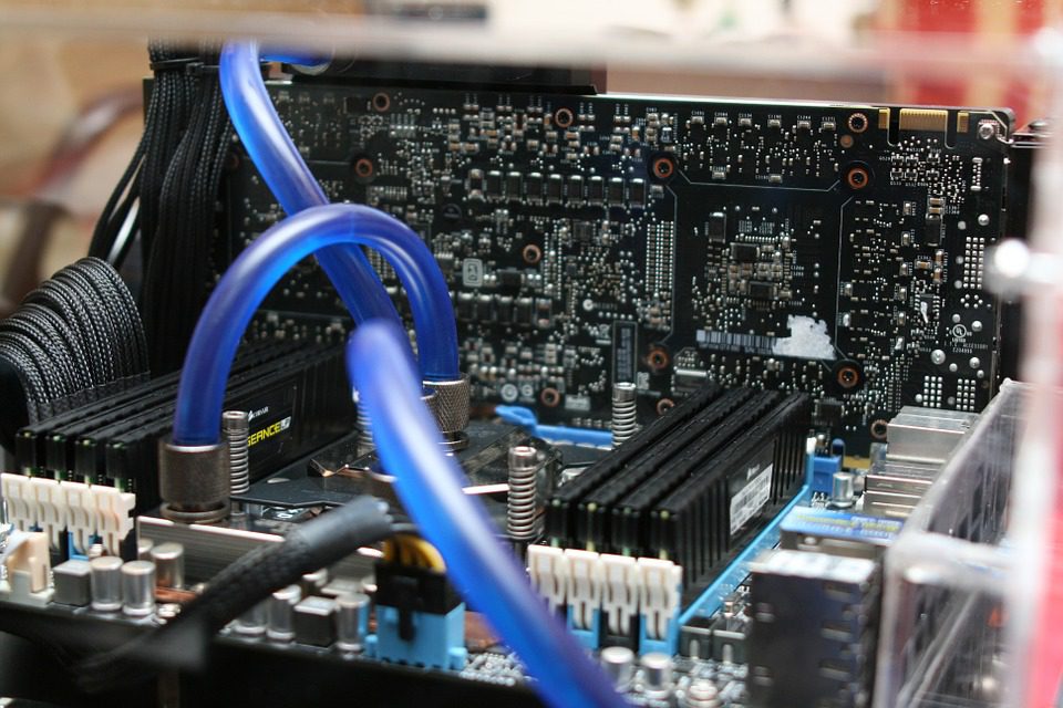
A motherboard is the printed circuit board containing the key parts of a computer. It facilitates communication between the different components of the computer, connects to external hardware, manages the video circuitry, and more. It is essentially the air traffic controller of your computer. Nothing else in your computer could work without the motherboard.
The motherboard doesn’t just roll off of an assembly line, ready to perform heroic tasks. Rather, it is assembled through a lengthy, painstaking process.
Here’s a closer look at the steps for creating motherboards:
1. Making the printed circuit board. The process starts with a sheet of fiberglass fabric impregnated with epoxy resin. It is known as a “prepreg.” The prepregs are stacked to the designated thickness, sandwiched between copper foil, and heated until they bond together and become stiff. (Copper is the metal of choice because it is especially good at conducting electrical current and heat.) This process creates the printed circuit board (or PCB).
2. Creating copper tracks. Once the board has been generated, it is laminated on both sides with a photosensitive coating known as photo-resist. After that, a transparent artwork is placed over the laminate. The artwork shows the design for the tracks and pads of the PCB. The board is then placed under ultraviolet light and dipped in a chemical solution. The copper underneath the design stays intact, while the residual copper is etched away through a high-pressure spraying process. The resulting assembly is called a “core.”
3. Stacking up the cores. The cores can now be stacked together, but a layer of prepreg must be inserted between each core and also on the top and bottom of the stack. This is necessary to shield the board from the pressure and heat needed to bond the stack together.
4. Drilling. At this point, holes are drilled in the board for mounting (bolting the motherboard in place within the computer), through-hole components, and vias, which make the electrical connections between the copper layers.
5. Electroplating. The vias need to be made conductive, and this process involves coating the board with a conducting metal (copper) and then a layer of tin. The tin keeps the copper from tarnishing and facilitates soldering (better than copper does).
6. Component mapping and solder masking. After this, the board is silkscreened to identify where parts should go. This also designates where solder should not go for the upcoming soldering process. Without this solder masking, the solder could be applied in unwanted areas and create problematic bridges between tracks.
7. Routing and testing. At this point, the boards are separated with a router. The same router can be used to drill non-plated larger holes and slots. The board is then tested to ensure that the electrical pathways are working as they should and are free of shorts. After this, the entire board is given a quality inspection to make sure that it meets basic specifications.
8. Component mounting. The most modern type of mounting is surface mount technology. With this process, solder paste is applied to the board in designated areas where the surface-mount components will be added. The paste holds the components in place so that the board can progress to the reflux soldering process. With reflux soldering, the board is heated to over 2000°C, enhancing electrical connectivity and allowing the solder to solidify. Larger components are not attached through surface mount technology, but through through-hole mounting. This uses pins that stick through the bottom of the board and are hardened and made conductive through wave soldering (molten solder washing across a board).
After this, the motherboard is tested, packaged, and built into a computer. The next time you fire up your personal computer, you’ll have a new perspective on the complex processes that account for its amazing capabilities.
