PCB manufacturing and design bring about a range of challenges, and one of the critical issues to tackle is signal integrity retention. When signals are transmitted on a PCB, they often suffer from distortion caused by quantization noise, signal noise, and other undesirable outcomes. Luckily, a powerful solution for tackling this issue is the implementation of a back drill PCB.

(freepik/Freepik)
What is Back Drilling?
High-speed PCBs present a multitude of challenges when it comes to maintaining signal integrity. However, a PCB assembly company can address these challenges effectively through meticulous architecture and well-executed production processes. One particular concern in high-speed architecture is the presence of transverse components, which are non-functional parts of the transmission. These components can significantly impact signal integrity.
Stubs, which arise from these transverse components, cause a reflection of signals from the stub end, thereby interfering with the original signal. To overcome this issue, you should employ Depth Control routing PCB techniques. This involves re-drilling the PCB with a slightly larger drill bit to eliminate the majority of the through stub.
The concept of back drilling entails creating an opening with a diameter slightly larger than the plated through-hole (PTH) in order to remove the conductive material from the stub. You should reduce the depth of the drilled back hole to a length of 10 mils or less. If the stubs exceed this length, signal reflections are generated, negatively impacting signal integrity.
Why is back drilling also referred to as control depth drilling?
The term “control depth drilling” is often used interchangeably with back drilling because manufacturers employ this technique to establish and regulate the depth of drilled holes.
Benefits of Back Drilling
Using back drilling on your PCBs provides a range of benefits:
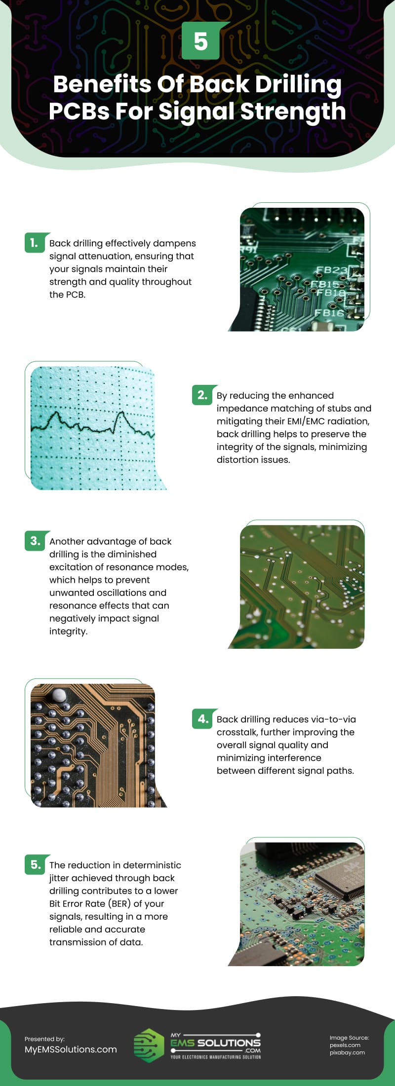
- Back drilling effectively dampens signal attenuation, ensuring that your signals maintain their strength and quality throughout the PCB.
- By reducing the enhanced impedance matching of stubs and mitigating their EMI/EMC radiation, back drilling helps to preserve the integrity of the signals, minimizing distortion issues.
- Another advantage of back drilling is the diminished excitation of resonance modes, which helps to prevent unwanted oscillations and resonance effects that can negatively impact signal integrity.
- Back drilling reduces via-to-via crosstalk, further improving the overall signal quality and minimizing interference between different signal paths.
- The reduction in deterministic jitter achieved through back drilling contributes to a lower Bit Error Rate (BER) of your signals, resulting in a more reliable and accurate transmission of data.
Limitations of Back Drilling
The back-drilling process presents limitations that require careful attention in terms of depth control. Inaccurate back-drilling machines can result in low tolerance, making it crucial to exert control over the back-drill depth.
Additionally, external factors such as drill-tip angle, drill resistance, contact between the cover board and the measuring unit, and board warpage can impact the back-drilling depth. Therefore, it is essential to choose suitable drilling methods and materials during production to achieve higher depth control for more accurate results.
Another important aspect is the accuracy control of back drilling. The chosen drilling method, board contraction and expansion characteristics, and equipment precision can affect the overall accuracy of the back-drilling process. Close attention should be paid to these factors to ensure the desired level of accuracy is maintained.
Example of Back Drilling
Let’s consider a scenario where there is a pathway from layer 1 to layer 12 in a 12-layer stack-up. However, the intended transmission is only between layer 1 and layer 3 signals. As a result, a through stub forms after layer 3 to layer 12, leading to the creation of high-frequency repetitions and reflections. These resonant frequencies can cause signal attenuation.
To address this issue, a PCB manufacturer will implement back drilling to remove the layer 3 copper plating up to layer 12, effectively reducing the duration of the stub. The back-drill PCB should have a wider diameter than the previous gap to eliminate the excess copper.
Here’s a valuable Design for Manufacturability (DFM) tip: The width of the PCB back drill should be slightly larger than the main drilling diameter. Typically, the diameter of the back pin is 8 mils larger than the primary pin size, with a preferred length of 10 mils. Try to ensure that trace and plane clearances are sufficiently high to avoid accidental back drilling in traces and planes adjacent to the backboard hole. We highly recommend maintaining minimum clearances of 10 miles for planes and traces.
What Are The Most Effective Alternatives to Back Drilling?
Buried and blind vias, laser-drilled vias, and alternative stack-up arrangements are some of the top alternatives that can effectively manage stub length and address the challenges associated with back drilling.
How To Set Up Back Drilling
Let’s go through the steps required to set up back drilling as follows:
- Choose the specific section where you want to apply back drilling. In this demonstration, we will focus on the RX segment within the Ethernet portion.
- Access the Design menu and navigate to the Stack Manager for the Layer option.
- Within the Stack Manager, locate and click on the Settings tab situated at the top right corner of the application.
- From the dropdown chart, select the Back Drills feature.
- Next, click on the Back Drill tab positioned at the bottom left of the panel. By doing so, the back-drill option will become visible, enabling you to configure various parameters related to back-drilling.
- If you need to add additional back drillings, simply tap on the plus key. Conversely, if there are any back drills you no longer require, you can remove them by selecting the bin symbol.
To conclude, back drilling emerges as a valuable technique utilized by PCBA manufacturers to address the challenges of signal integrity in high-speed PCB design. By effectively eliminating reflections caused by via stubs, back drilling ensures the preservation of the original signal. This process reduces stub length, preventing the generation of disruptive reflections.
PCBA manufacturers can rely on back drilling to deliver reliable and efficient PCBs that meet the stringent requirements of signal integrity. By embracing this technique, they can optimize the performance of their boards and enhance the overall quality of their products.
Infographic
PCB manufacturing faces challenges in signal integrity. Back drilling PCBs address issues by managing architecture and production. They create larger openings to remove stubs, ensuring clean signal paths. Proper setup is crucial. Back drilling optimizes performance, meeting demands for reliable data transmission in modern electronics.

Video

