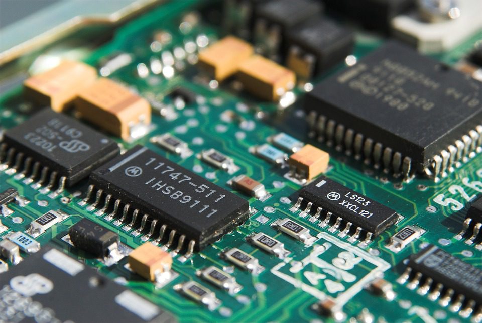
Although the average American may know very little about printed circuit boards, they would find it hard to live without them. PCBs are the workhorses of modern-day electronics. They are found inside of computers, printers, microwave ovens, cell phones, digital clocks, stereos, televisions, and more.

(Pixabay / axonite)
A PCB provides electrical connectivity using conductive tracks, pads, and other components that are etched from copper sheets. These components are laminated onto a non-conductive substrate. PCBs can be very simple and have just one copper layer. They can also be very complex, with capacitors, resistors, and other components on multiple, interconnected layers.
Printed circuit boards were not invented overnight. They are the product of many advances in electronics. Here’s a look at some of the milestones that have led to today’s high-functioning PCBs:
Electronic Circuit Making Equipment (ECME). This was a step in the right direction toward the printed circuit board. The technology could produce three radios per minute. Its inventor, John Sargrove, sprayed metal onto Bakelite plastic board.
Auto-assembly. This process came to consumer electronics in the 1950s thanks to the United States Army. Automated assembly changed the future of electronics circuits.
Point-to-point construction. Before printed circuits, we relied on point-to-point construction. This non-automated construction of electronics circuits used vacuum tubes and large sockets. The results were big, unwieldy circuits put together with screws and wire nuts. The contacts often corroded or became loose, and the circuits often failed. Because these circuits had to be assembled manually, they were more costly and more prone to wiring errors.
Through-hole technology. Printed circuit boards used to be dotted with holes to accommodate the wire leads that came from each electronic component. The leads were sent through the holes and soldered to the PCB trace. This changed due to the above-mentioned auto-assembly process. Through auto-assembly, the leads were inserted into an interconnection of copper foil and dip soldering. This process was the precursor to lamination and etching that is used today.
Surface mount technology (SMT). Through-hole technology is still used for making connections between multi-layer printed circuit boards. However, surface mount technology allows for more efficient component connections and, ultimately, smaller boards with greater functionality and lower production costs. Surface mount technology came into use in the 1980s.
Wave soldering. Clumsy, error-prone manual soldering was replaced by automatic soldering. Referred to as wave soldering, a printed circuit board passes over a wave of molten solder, and the components are automatically soldered.
These are just a few of the advances that brought PCBs to where they are today. The future holds many exciting possibilities as printed circuit boards continue to evolve. As a sneak peek, think 3D-printing of PCBs and “green” printed circuit boards made of recyclable paper.
