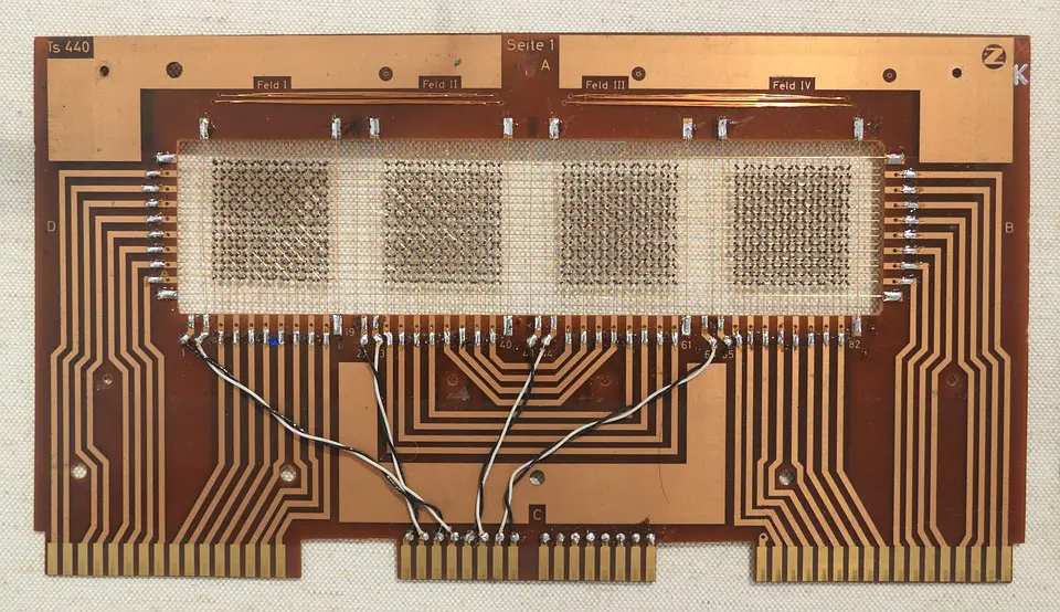
All printed circuit boards may look similar to the untrained eye, but there is a world of differences between boards, depending on their intended use. The techniques used to create the boards are different, too, but most involve some basic steps.

(Pixabay / olafpictures)
Printed circuit boards fuel the electronics industry. They are responsible for keeping cell phones, digital clocks, computers, printers, televisions, home appliances, and gaming devices running. They’re also critical in medical devices and aircraft.
The simplest boards are single-layered, meaning that they contain copper tracks on just one of their surfaces. More complex boards can be double-sided and multi-layered.
Though there are nuances in each stage of production, here’s a look at the basic steps for manufacturing PCBs:
- Layout development: PCB development starts with the creation of the plots for mounting components (known as photo works). After that, corresponding proto plots are created. These schematic processes are then translated to the board. This is often done through Gerber data, which is a file format that is imprinted on the board. The data from this format communicates design information, letting the engineers know the specifications for a designated board.
- Material gathering: Based on the layout, the proper manufacturing materials are gathered. Copper is the predominant material for most boards.
- Drilling: Tooling equipment is used to drill holes in the board in the places where components will be attached. There are a couple options for drilling, including through-hole drilling or surface mount technology.
- Plating: In this step, a board will be plated with different materials. These materials could include solder, tin, or gold. This coating protects the copper beneath from being worn away. The type of plating material will depend on the intended use of the board.
- Legend printing: A legend is imprinted onto both sides of the printed circuit board. The legend is critical in helping the engineers know how to build the PCB. It indicates which types of switches to use, component placement, test points, and more. Silk screening is one type of legend printing. Liquid photo and ink-jet imaging are other types.
- Greasing: The board must be greased so that it functions smoothly under pressure.
- Cleaning: The excess grease and any other residue should be removed through a cleaning process.
- Testing: Testing is critical for any board. Bare-board testing can help detect electrical shorts or ferret out any missed or improper connections. Rigorous testing solutions ensure top performance.
At EMS Solutions, we don’t cut corners. Each step of the manufacturing process is executed with top precision. Contact us to find out what makes our company one of the country’s highest quality PCBA manufacturers.
