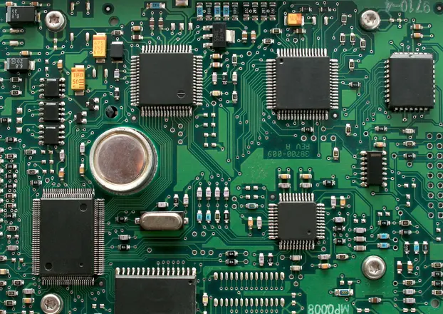
Printed circuit board assembly, or PCBA, involves intricate detail and manufacturing steps. Let’s explore a few.

1. Before starting any manufacturing process, you have to be operating within a completely sterilized area. In this case even, the air that circulates in the area must be very treated.
2. The first step in manufacturing a circuit board starts with the unraveling of woven fibers of glass that are fed into a processing component. Here, a resin of epoxy in applied. The glass fiber is then rolled to desired thickness while the excess resin is taken off it. Then, the glass fiber is baked in an oven and cut into parts which are than piled with copper foil in between to act as a gluing agent. The fibers are then tightly pressed and go through temperature and pressure testing to form a tight substrate.
3. Holes are then drilled into the substrates based on the predetermined design. After which, the drilled substrates are cleaned, and the inner parts of the holes are plated with copper which will act as a conductor.
4. Copper is then plated on the substrates’ surface in a predesigned pattern.
5. Contact fingers are then fixed in. The fingers are then plated with nickel, tin, gold or whatever is applicable.
6. The coating is then re-cooked in the oven to make it firm.
7. Epoxy is laid as a protection to the circuit as the assembly goes on.
8. Next, these panels are cut to the desired sizes.
9. Additional soldering or assembly of other components is completed.
10. The last step is when circuit boards proceed through quality control inspection.
