If you’re into printed circuit board assembly (PCB) or looking to enter the industry, you may have heard about the printed wiring board (PWB). However, unlike PCB, the term PWB is much less widely known, despite its existence being vital to PCB production. Today, we will look at what a PWB is, how it’s made, and what makes it so crucial to PCB production.

(Brian Wangenheim / unsplash)
What is a Printed Wiring Board (PWB)?
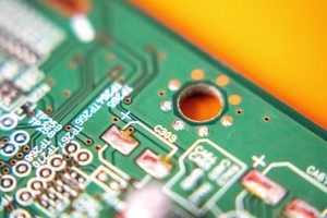
A PWB is a bare-tempered board on which components are installed to create a PCB. First developed in the 1950s, printed wiring boards are designed to allow the highest count of components per square inch. This means that one can build the boards to be more complex, better ventilated, easier to test, and configured to make them ideal for any electronic device.
The components affixed to the board’s surface are built in a reduced size to allow for a higher component density without detriment to the circuit’s electrical, thermal, and signal integrity performance.
The PWB is a substrate consisting of reinforced glass fiber and epoxy resin bonded onto a layer of copper foil. Known as FR4, it is the most common form of PCB substrate. Because it is a solid building base and is flame resistant, it allows components and traces to heat up with no damage.
What Is The Difference Between a Printed Wiring Board and a Printed Circuit Board?
The most significant and noticeable difference between the two is the use of components. As a printed wiring board is just the substrate formed and ready for component application, you can consider it an in-progress printed circuit board. Once the components and other circuitry are in place, the PWB becomes a fully-finished PCB.
During the earliest days of electronics production, the term PWB was more apt due to the use of the boards as connectors. Electronics engineers created the newer term to differentiate between a semi-finished and fully-finished PCB after the components became more widespread.
Production lines across the U.S. typically use the term PCB. In Japan, on the other hand, producers use PWB much more frequently because of confusion between an initial PCB and a complete PCB.
3 Factors that Can Affect a PWB’s Performance
Final product performance depends on the quality of PWB construction. There are many factors that PCB designers and assemblers must consider when designing the printed wiring board for their PCB. These include:
1. Operational speed
In the final product, the circuits created on a PWB will run currents from a power source through traces to the components and then back again. This is handled mainly by the copper traces built into the board; the substrate around them affects the signal strength and speed.
The substrate negatively affects the signal’s propagation time, known as the time of flight. Mathematically, it is inversely proportional to the square root of the dielectric constant of the substrate material. In layman’s terms, the thicker and less conductive it is, the more resistance the signal will face.
The lengths of the conductors through which the signal travels will also affect the time of flight. For a concise and fast design, assemblers must use shorter conductors. If the required performance is higher than 25MHz, then strip lines and micro-strips can supplement the conductors to boost performance.
2. Power consumption
Power consumption is a constant concern when building printed circuit board assemblies, and the problems can begin occurring as soon as the PWB stage. As the number of circuit gates increases, so will the power consumption. When designing a PWB, one must consider the ideal power supply and adjust the number of gates and the clock rate accordingly.
Further, you must also plan the ground return current flow of the traces when high-speed switching circuits are involved. Without the correct level of grounding, switched circuits can quickly lead to overheating, burnout, or disrupted the current flow.
In the cases of multilayer boards, you will need to fit a ground plane between each layer to keep resistance low. These will act as more expansive grounding areas and effectively disperse the return current.
3. Thermal management
PWBs themselves conduct heat inefficiently. The substrate itself absorbs and holds heat, meaning that you must build other methods into the PWB to disperse the heat buildup.
While FR4 is the best option for most circuits since it can absorb a decent amount of heat, higher-speed ones require a much greater capacity for thermal management. Fortunately, there are some ways to achieve this. You can use:
- Heat Sinks – These are designed to draw heat away from the board itself, allowing it to dissipate without affecting the circuit.
- Heat Vias – Also known as thermal vias, heat vias are small holes lined with a conductive element that draws the heat buildup through the board. On the other side, the space around the board can draw off the heat.
- Conductive Planes – Generally used with multilayer boards, conductive planes are a layer of conductive material laid between two layers. They absorb the heat from the surrounding boards, giving it a broader area to safely dissipate.
Incorporating any of these components into the PWB’s construction will provide a greater degree of thermal management and current and component usage. The choice of methods depends on the PCB plans and the number of layers.
Printed wiring boards represent a specific part of the PCB construction process. Their design is just as, if not more, important as the plans for the overall product. A poorly designed PWB will lead to a poor PCB. When choosing a PCB assembly partner, make sure to take the PWB quality into consideration.
Video

