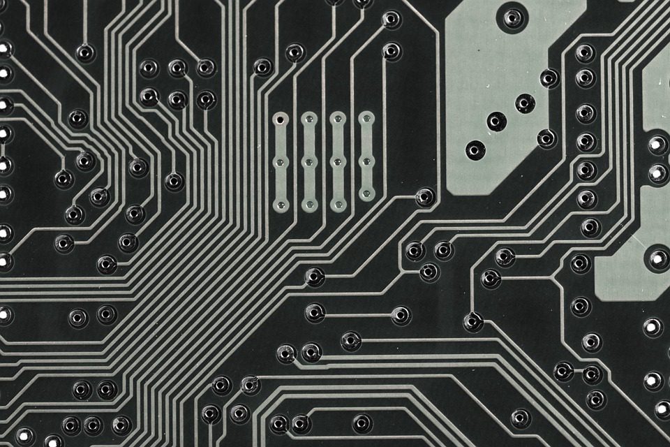
If you’re looking to shave time off of your prototype PCB fabrication processes, save money, and reduce error potential, SMT stencils are a must.

(Pixabay / blickpixel)
In a nutshell, SMT stencils are used for applying all-important solder paste to the PCB layout. Here’s a closer look at the process. Each PCB has many components. A stainless steel laser is used to cut through materials and create apertures for each of these components. After the cutting is done, the SMT stencil will be placed on top of the board. Then comes the solder paste. It will be applied to the stencil, and a squeegee will be used to make sure that it is distributed evenly over the openings where the components will go.
The stencil helps eliminate fuss and mistakes. The alternative is hand soldering, but this clumsy process can be fraught with human error. If you apply too much solder paste, you could end up with the following problems:
- Bridging: With bridging, excessive solder causes two or more pads to become connected, creating a bridge.
- Balling: Too much solder can result in the solder balling up.
- Tombstoning: This error will cause your PCB components (usually resistors or capacitors) to lift up from the pad on one end so that they look like a tombstone in a graveyard.
The SMT stencils will help keep these common problems from occurring. These stencils will also save you money because they are much cheaper than production stencils. And best of all, they’ll free your team up from having to worry about applying the right amount of solder into every nook and cranny.
Whether you are fabricating PCBs that are multi-layered, single-sided, or double-sided, SMT stencils can save you stress, time, and money and help you create a far more efficient product in the end. For help with questions about PCBA layout or surface mount assembly, contact EMS Solutions. We provide design collaboration to help you and your team achieve the highest quality output.
