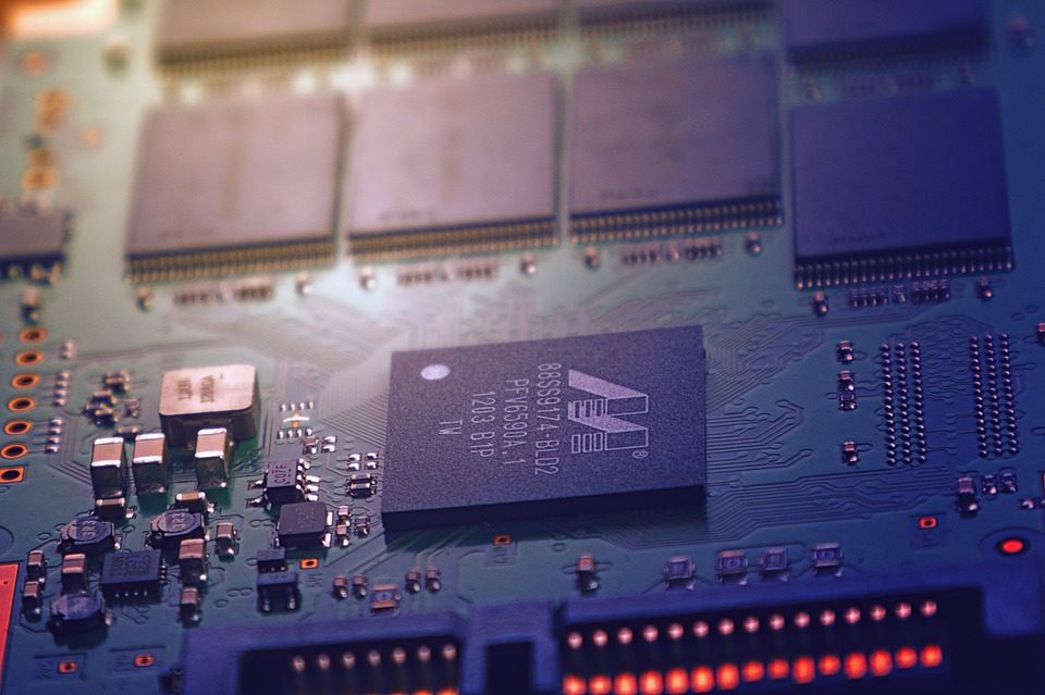
As semi-conductors grow more and more complex, the methods for packaging the technology are changing. These new methods are named according to their mounting style.

(Pixabay / jplenio)
Through-Hole Mounting: This method uses lead wires that are fed through the board through holes in a multi-layer printed circuit board. The leads are permanently mounted using soldering.
Surface Mounting: This mounting method is a newer iteration and accommodates the rapidly increasing number of pins in integrated circuits. Consumers want smaller devices that weigh less, and surface mount technology fits the bill. Rather than relying on hole mounting, SMT allows leads to be soldered directly onto a PCB surface. It facilitates much greater capacity in a limited space.
The soldering methods for surface mount technology are different than those required for through-hole technology. Here’s a closer look at what happens to a printed circuit board as it undergoes surface mounting:
- An SMT screen printer coats solder pads with paste. Surface mount circuit boards have hole-less pads called solder pads. For surface-mount circuit boards, these pads are flat and are usually made of gold-plated copper, but they can also be made of tin. A surface mount technology screen printer is used to cover these pads with a paste that is an amalgam of solder and flux.
- SMD components are added to the PCB. Once the solder paste has been applied, the PCB is placed on a conveyor belt. Electronic components are picked up by a machine and applied to the solder pads.
- The PCB is sent to the reflow oven. The oven subjects the PCB to multiple phases. The first part of the oven pre-heats the PCB, exposing it to gradually-increasing temperatures. If you were to put the PCB directly into a full-heat oven, the components might break under the thermal stress. The second phase sends the PCB into temperatures that are hot enough to melt the solder paste. This has the effect of soldering the pads to the circuit board. If a printed circuit board has two sides, it will need to pass through the reflow oven twice.
- The PCB is cleaned off. Now that the board has weathered the reflow oven for proper soldering, it must be washed to remove debris. If reside is not removed, it could cause the component leads to malfunction. There are a number of different solvents that can be used to clean the PCBs, including fluorocarbon and hydrocarbon solutions.
- The PCB is inspected. The human eye can give the PCB a final viewing to ensure that everything is aligned and that the solder is properly bridged.
- The component is sent for testing. Once the PCB passes the visual inspection, it can be sent to testing to make sure that it functions properly.
Ninety percent of technologies now rely on surface mount technology as an invaluable packaging method for the rapidly-evolving electronics industry.
