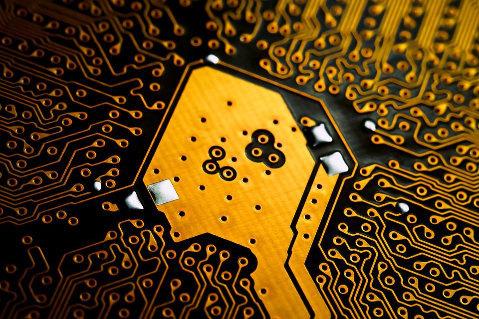
Who would have guessed that a tiny printed circuit board could help fuel a space station? PCBs continue to astound as they evolve at a rapid pace. What was once a pair of printed wires you had to maneuver is now a small chip you can hold between two fingers.

(Pixabay / 16946559)
Structure and evolution of PCBs
Learning, analyzing and designing electrical circuits becomes easy with schematics, in the form of symbols and lines. Symbols on a schematic depict components of a circuit like capacitors or resistors whereas lines represent pathways supplying electrical current to the symbols. However, schematics are only a diagram and cannot perform essential functions like blinking an LED light. To accomplish more with this visual design and take it into the physical realm, you have to use a printed circuit board (PCB).
Printed circuit boards are built on a flat, sturdy and insulated material with conductive structures on each side. These conductive structures also make geometric designs on the board. The long, thin lines represent interconnections, whereas other shapes represent the symbols or connection points for components.
PCBs have evolved in many ways since their entry into the electronics world. Developments in PCB designs have made these boards reliable and useful for modern-day projects. This can be seen from the fact that printed circuit boards power the majority of technological devices that rely on electronic components to function, including smartphones, computers, consoles, and more.
To learn more about PCBs, let’s explore how this board changed over the course of its lifespan:
Beginning Design of PCB
The second half of the 19th century brought major technological advancements. After the Civil War, cities in the East Coast and Midwest got electrical power while the usage of coil and heat was put to an end. Power grids connected neighborhoods and cities to electricity and oil was demoted to fuel until automobiles came around.
With readily available electrical power, bright minds introduced telephones, cameras and light bulbs. Although PCBs did not debut in this era, these developments set a foundation for their eventual development in the late 19th century.
1900s – 1950s
German inventor Albert Hanson filed for a patent for his PCB device in 1903. It was a flat conductor that did not attract much interest from inventors. The actual concept of a modern circuit board emerged in the 1920s and anything could be used to form its base material (even wood). It was a functional circuit board because you could drill holes in it and lay the wiring. Nuts and bolts were used to hold the board together, so you can say that its design foreshadowed the modern circuit board design.
The 1950s saw a rise in the use of other materials like resins in the circuit board base. Circuit boards of that time were one-sided where the wiring was laid on the inner side. It improved upon the bulky wiring of the past designs and was lightweight. Jules Andrus and Walter Bond at Bell Laboratories adapted photoengraving or photolithography for drawing patterns on circuit boards.
Later in 1957, Jay Lathrop and James Nall of the US Army’s Diamond Ordnance Fuse Laboratories
patented photolithographic methods to create miniature circuit boards. Photolithography was also used to etch holes in silicon wafers. The US then launched ‘The Process of Assembling Electrical Circuits,” which listed the modern ways of assembling a printed circuit board – a breakthrough in the world of PCBs.
Here is the process they followed:
- Draw the wiring pattern required for your device
- Photograph the design onto a zinc plate
- The zinc plate could then be used as a printing plate
The 1960s saw more options in circuit designs and better techniques that could prevent these boards from corrosion.
Multilayer PCBs also made an appearance in this time until engineers started reducing the size of circuit boards. In the 1970s, hot air soldering methods helped PCB designers to create smaller boards so that they could be installed in a wide range of devices.
Further Size Reductions in the 1980s
Surface mount assembly made it easier to further reduce the size of the circuit boards. It started becoming a norm in the 1980s and the through-hole method diminished to fit the circuit boards in smaller spaces. Computer-Aided Manufacturing then became a popular practice in the 1990s, resulting in the development of more complex circuit boards. In 1995, High-Density Interconnector PCBs featuring smaller lines, reduced weight and size made an appearance.
2000 and Beyond
Onwards from this phase, all older designs became outdated and defunct. Flex and rigid PCBs became more affordable and common to use in a multitude of technological devices. Now we’ve come to a point where the size and weight of a PCB is not a challenge. As we enter into the era of ‘smart spaces,’ manufacturers will be able to fit a PCB into any system with ease. There are so many innovations that could not have been possible without a PCB, and more awaits as these boards become even more sophisticated and efficient.
