DV/DT in electronics provide a deeper understanding of power semiconductor devices. These devices are akin to fast-acting switches, turning on and off rapidly—thousands of times within a single second. The swifter their action, the more dramatic the voltage and current changes become, which is precisely what DV/DT and DI/DT measure.

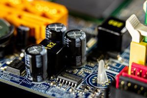
(Sergei Starostin/Pexels)
What does DV/DT imply?
DV/DT represents the rate of voltage change over time. It’s calculated as the change in voltage (delta V or ΔV) divided by the change in time (delta t or Δt). In practical terms, the DV/DT rating of a semiconductor device indicates the maximum voltage rise rate that won’t cause the device to conduct unintentionally.
DI/DT, similarly, is the derivative of current with respect to time. The DI/DT rating signifies the maximum permissible rate of rise of anode to cathode current that the device can handle without suffering damage. Exceeding this limit can create localized hot spots and potentially lead to semiconductor failure.
DV/DT in Specific Devices
- BJTs: In BJT circuits, DV/DT controls the voltage rise between the collector and emitter. A snubber circuit here limits the voltage increase during the turn-off phase to prevent damage.
- MOSFETs: DV/DT in MOSFETs is about controlling the drain-source voltage during switching. High DV/DT can cause issues like overshooting and oscillations due to interaction with circuit parasitics.
- Thyristors: For thyristors, DV/DT is about the anode to cathode voltage change when off. Exceeding the DV/DT limit can cause false triggering from internal junction capacitance.
DI/DT in Semiconductors
DI/DT, the rate of current change over time, is equally important. Exceeding the DI/DT rating in devices like thyristors can lead to hot spots and failure. EMS companies often manage this by controlling the speed of current rise during the turn-on phase.
Managing DV/DT with Snubber Circuits
To control DV/DT, snubber circuits are used. These circuits, made up of resistors and capacitors, help prevent sudden voltage increases across the device. They’re key in reducing issues like high-voltage transients, switching losses, and electronic noise.
DV/DT in Triacs: Managing Reactive Loads
Consider the behavior of a triac when the current drops below the holding current IH. In a purely resistive load, the triac stops conducting at the end of the sine wave cycle, where voltage and current are in phase. In inductive loads, there’s a lag between current and voltage.
When current falls below IH, the voltage may have risen with the opposite polarity. This sudden stop in current flow creates a significant DV/DT across the triac, potentially leading to self-triggering and uncontrolled conduction. To mitigate this, operators often use an RC network parallel to the triac.
Understanding DV/DT Rating in SSRs
The DV/DT rating of an SSR is a key factor. It shows the highest anode voltage rise rate that doesn’t push the SSR into an unintended conduction phase without a gate signal. This rating is crucial; exceeding it can unintentionally turn the SSR on, a condition known as false triggering.
Importance of DI/DT Rating
The DI/DT rating, defined in amperes per microsecond, controls how fast the current can rise during the SSR’s activation. The current increase can be too swift if the DI/DT exceeds the recommended limit. This uneven distribution can cause hot spots near the gate connection, where the current is most concentrated. These hot spots elevate the semiconductor’s junction temperature, potentially leading to irreversible damage.
Controlling DV/DT and DI/DT in SSRs
SSRs often integrate an RC network or a snubber circuit to manage these values within safe limits. This is particularly vital in inductive loads, where the DV/DT can easily surpass safe thresholds. For instance, Celduc’s Solid State Relays like the Zero-cross (SO8, SA/SU8) and Random or Instantaneous (SO7, SU7) are designed with these features, making them adaptable to various loads.
For capacitive loads, regulating DI/DT is crucial. Adding an inductor in series with the load can accelerate current changes. Celduc’s series, such as SO8/SU8/SGT8, utilize specific technologies to reduce trigger voltages and adapt to sudden current shifts, especially in capacitive loads like batteries and power supplies.
Locating DV/DT and DI/DT Specifications
These maximum DV/DT and DI/DT values are typically found in the product data sheets. For example, a DV/DT specification of 500 V/μs means the voltage can rise by 500 volts every microsecond. Similarly, a DI/DT rating of 50A/μs indicates a permissible current rise of 50 amperes per microsecond. Staying within these limits is crucial for the SSR’s safe and efficient operation.
Negative Effects of High DV/DT and DI/DT
Parasitic Characteristics in Circuits
The rapid switching speeds of DV/DT and DI/DT bring to light the “value” of parasitic characteristics in circuits. For example, a DI/DT of 12A/ns can cause a voltage drop of 12V at 1nH, and a capacitance of 12V/ns at 1pF can generate a current of 12mA. These parasitic parameters can be much larger in power main loops, posing significant challenges in circuit design.
Implications for EMI Radiation Spectrum
Excessive DV/DT and DI/DT affect the circuit’s internal dynamics and broaden the EMI radiation spectrum. You must carefully consider this factor in power circuit design to ensure compliance with EMI standards and maintain the efficiency of the power devices.
Conclusion
DV/DT shapes the way electronic systems perform and endure. By effectively managing these rates, EMS solutions providers can ensure optimal performance and longevity of devices.
Video
Infographic
DV/DT in electronics offers insight into power semiconductor devices, which act as fast switches, turning on and off rapidly. The speed of their action results in significant voltage and current changes, measured by DV/DT and DI/DT. Learn more in this infographic.

