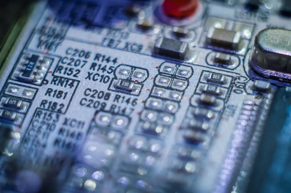
Inside almost every electronic device is a printed circuit board assembly (PCBA). It consists of various components attached to a board that is usually coated in a green color. This whole assembly is the heart of a machine’s electronics system. The green board where the components are attached is called the printed circuit board (PCB). The PCB is the core and base of the PCBA.

(Pixabay / y6uca)
Printed Circuit Board and its Layers
The PCB is manufactured separately from the PCBA. It consists of at least one layer of copper substrate, which is etched to form lines across the PCB. At intervals are holes where the various components are inserted or soldered. The components include capacitors, resistors, IC units, and transformers. It may even be connected to another PCB via a connector. The copper substrate serves as the electrical wiring for the board.
The PCB can have a single, double, or multi-layered substrate. It can have as many as a dozen layers. It can also be categorized as a rigid, flexible, or flex-rigid board. Besides the substrate layer, there are other layers on the board. A PCB can be single- or double-sided. A single-sided PCB has a copper foil layer on one side only, whereas a double-sided PCB has two sides with copper traces. For the PCB to be useful, electronic components are soldered onto it. Soldering makes use of a solder mask, which shields the copper layer and gives the board its signature green color. This is a non-conductive layer that ensures that the copper traces are not unnecessarily soldered on, thereby creating a short circuit. The solder is a small weld, which connects the component to the board. This should not be touching the other copper lines.
The last layer is a silkscreen. This details the actual components of the board. It is used to detail which components should be put in specific holes. It can also be used to write important information on the board.
Assembly Processes
The PCBA is the finished product after the electronic components are placed on the board and soldered. This process uses two methods: surface mount technology (SMT) and through-hole technology. Through-hole is the traditional method for placing components. The component’s legs are inserted through the hole on the board and soldered on the other side of the board. SMT, on the other hand, uses automated welds, which solder the components on only one face of the board.
The SMT method has become very popular in recent years because the board doesn’t need to be soldered on the other side. However, the main advantage of SMT is that it can be coupled with an AOI (or automated optical instruction) to enable quality assurance procedures to be expedited rapidly.
The whole manufacturing process can be divided into two, with different sites for the PCB and the PCBA. Some manufacturers can fulfill a full turnkey manufacturing solution for their clients. This includes sourcing materials, PCB manufacturing, PCB assembly, automated inspection, visual inspection, and final testing.
The PCB and the PCBA are distinct, but they represent two sides of the same manufacturing process.
