PCBs are critical components for various electrical devices and industries. However, a lot of buyers aren’t aware that PCB thickness can play a significant role in designing the ideal board for their needs. In some cases, the printed circuit board manufacturer may ask you to choose between standard and minimum PCB thickness, and your answer will help them tailor their processes to your design.

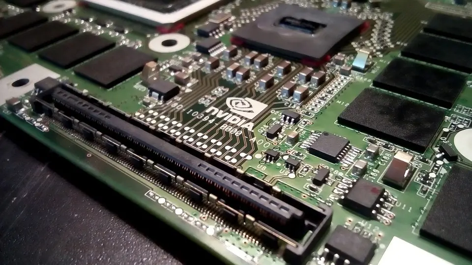
(Pixabay / JacekAbramowicz)
With that in mind, here’s a look at the two options for PCB thickness and how to decide what level you need.
What Is the Standard Thickness for Printed Circuit Boards?
Several vendors claim that the standard thickness for PCBs is 0.062 inches, or around 1.57 mm. While there’s some truth in their statements, these were the dimensions that were used in the earlier times of PCB fabrication. Hence, 1.57 mm can be regarded as the historical thickness for printed circuit boards.
Today, PCBs are designed to be much bigger and thinner than the historical standard. In fact, it’s more accurate to state that there is a range of standard or common PCB thickness options available. Some vendors, for example, use 0.0079 inch (0.2 mm), 0.020 inch (0.5 mm), and 0.016 inch (0.4 mm) thickness for the boards. Others will use 0.093 inch (2.36 mm) and 0.125 inch (3.175 mm) for the purpose. Based on your selection of the assembly line and PCB fabrication, you may get the option to buy boards with other dimensions.
What Is the Minimum Thickness for Printed Circuit Boards?
Simply put, minimum thickness PCBs are used to describe circuit boards that are much thinner than standard PCBs. For the majority of PCBs in existence, the minimum thickness is 0.2 mm. Because of the rising market demand for thinner electronics, there has been an increase in demand for thinner printed circuit boards such as 0.5 mm, 0.4 mm, and 0.2 mm boards. These can be used in SIM cards, sensor cards, and other similar components.
It’s worth mentioning that printed circuit boards are a work of several layers including epoxy copper and prepreg, dielectric cores with coating. Several kinds of PCB thicknesses can be attained through a mixture of prepreg sheets and varying core thicknesses. However, the manufacturer needs to use a single layer of the core to achieve a minimum thickness, which restricts the number of copper layers to double units. A higher quantity is only achievable by adding more prepreg and core layers.
To create mechanically functional PCBs, it’s critical that manufacturers distribute layers evenly with an odd quantity of dielectric layers and an even quantity of copper layers. Hence, boards with a larger quantity of layers can cut their overall thickness by leveraging thinner core options.
With all that said, those opting for very fine thicknesses may be left with a limited choice of surface finishes. Why? Because most surface finishes follow a different build process based on the production technique and material properties. For example, the gold finish (standard immersion) in most factories support the 0.2 mm PCB thickness, while “Lead Free HASL” is only compatible with 0.6 mm thickness. Likewise, immersion silver and tin should have 0.4 mm as the minimum PCB thickness.
How Can I Specify the Thickness of My Printed Circuit Board?
This can be done with the help of a trace width calculator. By entering all the necessary specifications on the board and following the instructions, you’ll get a fair idea of the ideal thickness.
Of course, you’ll need to know things like the solder mask thickness, the prepreg thickness, and what mm you want for the final result. It’s possible for the calculation to show hundredths of a millimeter to deliver an accurate measurement.
Keep in mind that a number of manufacturing and design factors will also be used to determine the printed circuit board’s thickness. The manufacturing concerns usually include copper thickness, layer count and drill hole equipment. The design factors, on the other hand, include signal types, the quantity of PCB layers, board materials, copper thickness, and the operating environment.
What Thickness Should I Go with?
When finalizing the thickness for your PCB, consider the following factors:
Flexibility
Thin boards have better flexibility than their thick counterparts. Also, thick boards can be heavy.
Weight
The weight of the PCB is a critical factor. Thinner boards give off a lighter feel. However, heavier devices demand PCBs with greater weight because thinner boards are prone to breaking.
Impedance matching
The thickness of the PCB defines the thickness of the dielectric. The latter is what helps achieve impedance control.
Area
See how much area is available for you to work with. Thinner PCBs take up less space, so they’re ideal to use in smaller electronic devices.
Cost
Last but not least, you need to compare the costs of standard thickness PCBs and minimum thickness PCBs. While utilizing non-standard thicknesses can bring benefits in the shape of a thinner product and better electrical performance, you can expect increased production costs. The most cost-effective PCB thickness is the standard 0.063 inch (1.6 mm). The usage of multiple layers also raises the cost due to additional processing steps and production material.
Final Verdict
While both PCB thicknesses have their unique set of benefits, it’s best to choose the standard route if you’re working with regular or large-sized devices. Using this option will most likely result in less expensive and quicker production of your boards. However, if you go with a minimum thickness PCB, then you should make sure there’s enough space inside the board to accommodate your decision, and the overall design offers a good chunk of flexibility.
