
High-speed PCB design challenges even experienced engineers. As devices push faster data rates, proper routing becomes the difference between reliable performance and frustrating signal problems. When signals travel at high frequencies, the PCB layout itself becomes part of the circuit.
For electronic manufacturing service providers, mastering high-speed routing techniques directly impacts product quality and reliability. Poor routing decisions lead to crosstalk, reflections, EMI issues, and power distribution problems that can be difficult to troubleshoot after manufacturing.
This guide shares practical high-speed PCB routing strategies developed from real-world electronic printed circuit board assembly experience. We’ll cover essential techniques for controlling impedance, optimizing trace geometry, managing return paths, and minimizing noise—helping you design boards that perform reliably on the first production run.
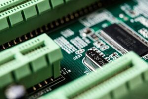
(freepik/Freepik)
Understanding High-Speed PCB Routing
High-speed PCB routing techniques manage circuit designs where signals change state rapidly—typically in the megahertz (MHz) or gigahertz (GHz) range. The challenge lies in delivering these fast signals to their destination without degradation or interference.
As frequencies climb, physical effects begin to intensify:
- Inductive and capacitive coupling create crosstalk between traces
- Impedance mismatches cause signal reflections
- Return path discontinuities generate electromagnetic interference
Traditional PCB routing techniques that work for low-frequency applications simply fail under these conditions. Engineers must implement specialized high-speed PCB routing methodologies to maintain signal integrity.
A well-designed high-speed PCB minimizes signal loss, reduces interference, and optimizes power distribution to support stable operation.
Expert Tips for High-Speed PCB Routing
1. Optimize Layer Stack-Up for Signal Integrity
Start with your layer stack-up—it’s the foundation of high-speed signal performance. How you arrange signal layers, ground planes, and power planes directly impacts impedance control, noise immunity, and signal propagation.
Always place dedicated ground planes next to signal layers. This proximity creates low-impedance return paths for your signals. Similarly, keeping power and ground layers close together generates natural capacitance that helps distribute power evenly and suppress noise.
Don’t overlook your material choices. Different dielectric materials affect signal velocity and impedance calculations due to their varying properties. Maintain consistent dielectric thickness throughout your board to prevent impedance variations that can create reflections or distortions in your high-speed signals.
2. Control Your Impedance
Controlling your impedance helps prevent signal reflections that cause data integrity problems and signal loss. Three factors determine your trace impedance: width, dielectric thickness, and PCB material properties.
Use impedance calculators or PCB simulation tools to determine the correct trace dimensions for each board layer. Your goal is to maintain consistent impedance across all transmission lines, creating a smooth path for high-speed signals. Even small impedance variations can degrade signal quality at high frequencies.
3. Reduce Crosstalk and EMI Mitigation
Crosstalk occurs when signals on adjacent traces interfere with each other, leading to unintended noise and distortion. This is a common issue in high-speed PCB design, especially when traces run too closely together.
To minimize crosstalk, you should:
- Maintain proper spacing between signal traces to reduce inductive and capacitive coupling.
- Route differential pairs close together with uniform spacing to ensure they function as intended.
- Use ground planes and shielding techniques to isolate sensitive signals from high-noise areas.
Electromagnetic interference (EMI) presents another major concern in printed circuit board assembly. High-speed signals can act as radiating sources, causing interference with nearby components or external devices. Shielding techniques, such as using guard traces or ground vias, help reduce EMI susceptibility.
4. Minimize Signal Reflections Through Proper Termination
Want clean signals? Address reflections. They occur at impedance discontinuities and corrupt your data by creating overlapping waveforms.
Add series termination resistors at the source to absorb excess energy before it rebounds through your traces. For long transmission lines, try parallel termination at the receiving end—this stabilizes voltage levels and prevents ringing.
The goal is simple: create a smooth pathway where your signal’s impedance matches perfectly from driver through trace to receiver.
5. Consider Power Integrity and Decoupling Capacitors
Even the best signal routing fails without stable power. In EMS PCB assembly, power integrity deserves as much attention as signal integrity.
To deliver clean power:
- Replace thin traces with wide power planes that minimize resistance.
- Deploy decoupling capacitors strategically—small ceramics close to ICs handle high-frequency noise while larger caps support bulk current demands.
- Create the shortest possible path between power sources and high-current components.
Think of your power distribution network as the foundation supporting your high-speed signals. When voltage remains stable during rapid current changes, your high-speed signals can perform at their peak.
6. Avoid Sharp Bends and Right-Angle Traces
Sharp bends in PCB traces create impedance discontinuities, leading to signal reflections and EMI problems. Abrupt 90-degree angles can cause signal loss, especially in high-speed designs.
To prevent this, use 45-degree bends instead of sharp angles. In high-frequency circuits, arc routing smooths transitions and prevents interruptions. Keep high-speed traces short and direct to minimize signal path variations.
By maintaining smooth and continuous trace routing, you can improve signal integrity and reduce unwanted reflections.
7. Use Differential Pair Routing for High-Speed Signals
High-speed interfaces like USB, HDMI, PCIe, and Ethernet use differential signals to improve data transmission. These signals rely on two complementary traces carrying opposite charges.
To ensure signal integrity, match trace lengths to prevent timing mismatches. Keep spacing consistent to control impedance and avoid distortion.
It’s also important to be mindful of power plane gaps. Crossing these gaps breaks the return path and weakens signal integrity. Use a continuous reference plane to maintain stability and prevent interference.
How High-Speed PCB Routing Impacts EMS PCB Assembly
For PCBA EMS manufacturing and assembly, high-speed designs require precise manufacturing techniques and engineering. Fabrication must meet tight tolerances, support multilayer stack-ups, and undergo high-frequency testing to verify performance.
Use time-domain reflectometry (TDR) and vector network analysis to confirm impedance control. Conduct design for manufacturability (DFM) reviews to catch issues before production, preventing revisions and improving efficiency.
These steps help you build high-speed PCBs that meet industry standards and support advanced electronic systems.
Conclusion
High-speed PCB routing shapes how a circuit performs, not just in theory but in real-world conditions. However, getting it right takes more than following best practices. Small miscalculations in trace geometry, impedance control, or power distribution can introduce unexpected failures.
Partnering with an experienced electronic printed circuit board assembly provider ensures that high-speed PCB designs are optimized for manufacturing, testing, and long-term reliability.
Frequently Asked Questions (FAQs)
1. What is high-speed PCB routing?
2. Why is controlled impedance important in PCB design?
3. How does PCB layer stack-up impact high-speed signal integrity?
4. What is the best way to reduce crosstalk in high-speed PCBs?
5. How do differential pairs help in high-speed PCB routing?
6. What are the most common causes of EMI in PCB design?
7. How can I prevent signal reflections in my PCB design?
8. What role do decoupling capacitors play in power integrity?
9. Why should I avoid right-angle bends in PCB traces?
10. How do EMS PCB assembly providers ensure high-speed PCB performance?
Video

Infographic
High-speed PCB design comes with unique challenges, where layout decisions play a crucial role in performance. At high frequencies, your PCB acts not only as a physical platform but also as a vital part of the circuit itself. Check out this infographic for expert tips on high-speed PCB routing.
